 Delete Article!
-
062010. 07
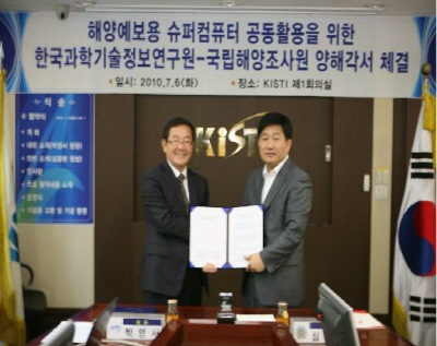
No. 50 View. 24058 Supercomputer will be used in developing forecasting model for massive marine disaster and climate changes. Korea Hydrographic and Oceanographic Administration (KHOA) and KISTI agreed to cooperate in utilizing national supercomputing resources and science and technology information. KHOA is in charge of national marine information and its service and it will use KISTI supercomputer to develop high-resolution marine forecasting model necessary for precise marine weather forecasting.
-
182010. 06
No. 49 View. 24692
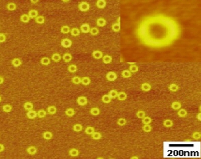
POSTECH develops nano-size 'doughnut' structure assembly
Technology to allow for synthesis of nano-size metal; chosen as notable study by Nature journal World-renowned chemistry journal 'Angewandte Chemie' carries study on front cover (Photo)Doughnut-shaped nanostructure assembly. Korean scientists have developed a new polymer nanostructure in the shape of a doughnut that is consistent in size, and is different from nano-metal particles of different shapes, including globular, cylindrical, disk and spiral shapes. Pohang University of Science and Technology (President Baek Sung-gi) said on June 11 that its research team led by Profs. Chang Tai-yun and Huang Hai-ying at the Brain Korea 21 molecular science initiative had developed a technology that allows for the production of nano-metal particles by employing as nanotemplate doughnut-shaped molecular assemblies that are consistent in size through the use of spontaneous self-assembly of diblock copolymers. Chang's team succeeded in creating a pure, consistently sized, doughnut-shaped nanostructure assembly (ring-closure products of rod-shaped micelles) based on a nanostructure assembly that was poor in utility due to the uncontrollability of its structure and size? by applying diblock copolymers with a low glass transition temperature, and a selectively reacting solvent mixture. The new structure assembly is drawing keen attention because it not only maintains the structure in the solvent mixture for several months, but also allows the nano-metal particles, which were created through careful manipulation of their size and shape, to be inserted into a specific location of the nanostructure assembly. If researchers synthesize nano-metal particles, which can be created to be consistent in size and shape, they can generate a new nano-compound of sophisticated shapes much more easily than via conventional methods.Moreover, since it allows researchers to easily generate a nanostructure assembly that is consistent in size, the technology is expected to make major contributions to applied research in related fields, including the development of next-generation nano-scale memory devices. The study was selected as the "VIP" and cover thesis in the latest issue of Angewandte Chemie, the world's preeminent chemistry journal published by the German Society of Chemistry (the Gesellschaft Deutscher Chemiker). The study was also introduced as a 'notable study' in the polymer chemistry field in the 459th issue of the journal, Nature, reflecting the keen attention the technology has attracted from international academia. (Photo)From left: Prof. Chang Tai-hyun, Prof. Huang Hai-ying (lead author), Ph.D. candidate Jung Ju-eun, Dr. Park Hae-woong. ? Lim Eun-heeredant645 at hellodd.com[June 18, 2009] - - - - - - -Source - HelloDD.com -
152010. 06
No. 48 View. 24842
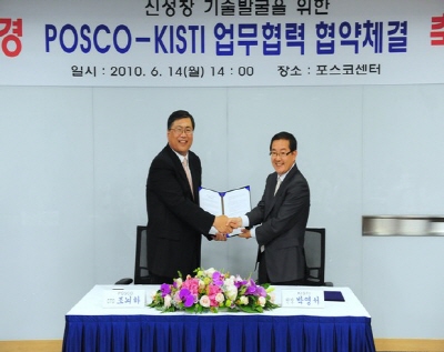
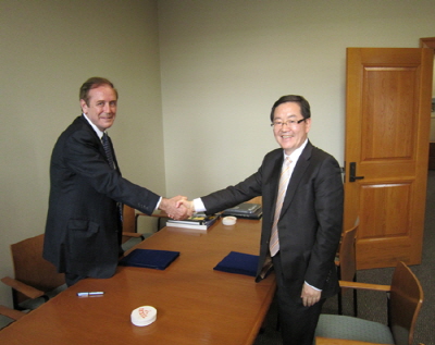
KISTI and POSCO signs MOU for New Growth Technologies
Dr.Park Y.S, President of KISTI shook hands with Dr.Cho N.H,CTO of POSCO at Posco center on June.14th. By concluding the MOU, KISTI and POSCO agreed to cooperate on developing new growth-engine technologies by exchanging in-depth analysis information on S&T. Both organizations will also co-host seminars and conferences on new technology and its future trend. -
082010. 06
No. 47 View. 23163
KISTI to get a tenfold increase of SME sales
- Find out 50 SMEs/Venture Businesses by 2015- Concentrated support for more than a 10-fold increse of SME sales in 10 years Korea Institute of Science and Technology Information(KISTI, President Park Young-seo) said on June 3 that it has developed a "10-10 Project" to pick out and foster small and medium enterprises in Dae-deok Science Town. 50 smaller businesses in the stage of rapid growth that have amount of revenue from $800 thousand to $ 8 million will be selected by 2015 and be intensively fostered step by step so that they could multiply more than 10-fold in their turnover after 10 years. Benefits the selected SMEs can receive are the following:▲ KISTI planner specialized in commercialization of technology▲ Support for the development of new item in association with Dae-deok Science Town▲ Provision of overseas market information jointly with Dae-jeon City▲ Automatically become a member of KISTI S&T Information Committee▲ Free provision of analyzed data Dr. Park Young-seo, President, said "The '10-10 Project' could support marketable future business and also contribute to economic growth and creating jobs of South Korea." -
012010. 06
No. 46 View. 23696
KISTI to Conduct "Safe Korea E"
KISTI conducted "Safe Korea Exercise(SKE)", safety training responding to crises and unexpected events such as a fire, earthquake, or a terrorist outrage, from May 27 to 29. KISTI trained staffs to ensure they learn how to respond to both natural and man-made disasters in a timely manner.It was the opportunity for the staffs to learn how to prevent disasters and reduce its impact in case of emergency situations through the simulated drills. -
082010. 04
No. 45 View. 23553
KISTI concluded MOU with UT Austin
KISTI(Dr.Park Young-seo,President) shook hands with the University of Texas Austin to supportKorean SMEs for entering US market. By concluding the MoU, KISTI and the university of Texas have agreed to exchange various consulting know-how for promoting technology commercialization of the products SMEs produced in Korea. Both organiztions will also expand their collaboration in supporting the export of SMEs who are unable to find partners in overseas due to their inexperience in marketing and localization. Both organizations will set up their branch office in each organization and will choose 2 innovative SMEs for providing `KISTI-UT Austin Tech2Global Market program. The university of Texas is located in Austin and is specialzed university for technology commercialization with GCG(Global Commercializtion Group) for marketing evaluation for SMEs and traning program for technology commercialization. -
302009. 12
No. 44 View. 23025
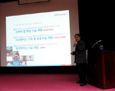
KISTI Hold Seminar on Technology Transfer
There was an annual presentation on technology transfer on December 21 at KISTI's headoffice in Daejeon. Hosted by KISTI, this presentation aimed to contribute to the advancement of industry by semantic information service technology transfer to enterprises. The researchers of Department of Information Technology Research made presentation on the product of their work, technology transfer procedures, and so on. -
212009. 12
No. 43 View. 23470
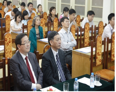
KISTI held "The 4th Korea-Vietnam International Seminar"
KISTI held "The 4th Korea-Vietnam International Seminar" in Hanoi, Vietnam from November 9 to 11. The seminar was held in cooperation with National Centre for Scientific and Technological Information(NACESTI) under the Ministry of Science and Technology of Vietnam. The seminar's aim was to promote executive understanding and joint research on political measures of Vietnam national S&T information and on the development of cyberinfrastructure R&D environment. Dr. Park Young-seo, KISTI's president, and researchers from KISTI's each research area, such as information analysis division, knowledge information center and supercomputing center, took part in the seminar and introduced their research performance and future high-tech trend they will pursuit in the future. -
092009. 12
No. 42 View. 25565
Korean scientists identify gene-generating 'anion channel' in Astrocytes
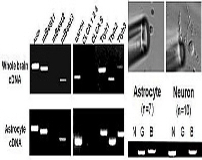
Korean scientists identify gene-generating 'anion channel' in Astrocytes. Dr. Lee Chang-joon at KIST's Center for Neural Science makes breakthrough Korean scientists have discovered the identity of the gene that generates 'Ca2+-activated anion channel (CAAC)' in Astrocytes. According to the Korea Institute of Science and Technology(President Han Hong-taek) on November 12, Dr. Lee Chang-joon at the Center of Neural Science at the Institute had discovered that the Ca2+-activated anion channel in Astrocytes is induced by a gene called Bestrophin. (Photo) Bestrophin genes exist in the brain cells, and are generated extensively in astrocytes in particular through a DNA amplification test. The surface of Astrocytes has various Ca2+-activated anion channels. These channels are said to play important functions in regulating the metabolic activities within cells, but nothing had yet been reported about which gene induces the channel. Along with nerve cells, Astrocytes are an important component of the nerve system. The study used imaging and electro-biological experiment methods. In short, it identified that anion channels are generated in cultured Astrocytes in mice brains, and brain cross-sections of conditional gene-regulation mice, especially the Hippocampal Astrocytes that exist on the hippocampus. Moreover, it discovered that most anion channels are induced by the emergence of Bestrophin, which had been known as the gene causing a hereditary visual disease called vitelliform macular dystrophy. (Photo) This picture shows the distribution of Bestrophin generated in mouse brain cross-sections through an experiment called "situ hybridization"(a method for identifying the location, distribution, and degree of emergence of a certain gene using DNA or NRA probes). Bestrophin is seen to be amply generated in the brain overall, and can be especially identified at the hippocampus. (Photo) Bestrophin genes are generated in astrocytes in mouse brain cross-sections, as presented through an immuno-staining experiment. Using imaging and electro-biological experiment method. Dr. Lee explained the achievement as follows: "Astrocytes had been only known for their role in assisting the neural transmission thus far, and were not considered very important. The result of the study is significant because it supports the hypothesis that Astrocytes not only help nerve cells maintain their functions seamlessly but are also related with diverse important metabolic activities, including damage and revival of the nerve system." He added, "The study is important in that we have laid the foundation for research to identify the roles of anion channels existing in the Astrocytes, and the mechanisms of biological activities within cells; moreover, it has opened up the possibility for the development of a great therapeutic drug for diverse brain diseases related with those functions." The study was published in the October 14 issue of the Journal of Neuroscience, an official journal published by the Society for Neuroscience in the U.S. ? Kim Jae-hojhkim at kofac.or.kr[November 24, 2009]- - - - - - -Source - ScienceTimes -
032009. 12
No. 41 View. 25077
Korean scientists develop technology for verifying infrared ray cameras
Korea Research Institute of Standards and Science develops evaluation device for large-sized infrared ray cameras to use device in Giant Magellan Telescope project An image of the evaluation device for infrared ray cameras. (Photo) An image of the evaluation device for infrared ray cameras using a performance measurement system. A Korean research team has developed a device that allows for the accurate assessment of large-sized infrared ray cameras, making Korea the third country in the world after the U.S. and Russia to develop the technology. The research team, led by Yang Ho-soon of the Center for Space Optics(Head Lee Yun-woo) at the Korea Research Institute of Standards and Science(President Kim Myung-soo), said on November 12 it had developed a device for evaluating the performance of large-sized infrared ray cameras in partnership with Korean research institutes and industry. The new device is capable of assessing whether an infrared ray optical system of up to 800mm in diameter can grade temperatures below the 0.01 degree Celsius level. (Photo) Dr. Yang Ho-soon, a research scientist at the Center for Space Optics. The evaluation device consists of an object section, which can adjust temperatures, and a "collimate device of 1meter in diameter" that renders the object to look as if it is far away by converting infrared rays emitted from the object section into parallel light rays, and software that operates the entire system and analyzes results of the measurement. Collimate devices generally use off-axis parabolic surfaces, which generate parallel light. Notably, in order to assess the performance of an infrared ray camera that uses a large reflector measuring hundreds of mm in diameters, a collimate device that is larger and better in performance than the infrared ray camera to be assessed is essential. Advanced countries are restricting the export of large collimate devices since they can be used for military purposes. Dr. Yang's team produced the device by changing the off-axis parabolic surface of 1 meter in diameter to less than 30nm(nanometers), using an off-axis parabolic surface processing system. Use of this system reduces the loss of material and the duration of processing by more than 75% compared with cases where conventional methods are used. Software for measuring performance evaluates the performance of an infrared ray camera by analyzing video images from the detector. It can evaluate virtually all performance elements of infrared ray cameras, including the capacity to divide temperatures to the minimum level, noise-equivalent temperature, signal-to-noise ratio, vision angle, and distance of focal point.Notably, the new off-axis parabolic surface processing system, for which patent has been filed, can be used for the production of aspherical surfaces larger than 1meter in diameter. The research team plans to expand the processing system and use it in the GMT (Giant Magellan Telescope). KRISC plans to participate in the project by producing seven 1.1 meter-diameter aspherical surface lenses jointly with the Korea Astrology and Space Science Institute. Dr. Yang Ho-soon said, "As we have domestically developed a device for evaluating the performance of large-sized infrared ray cameras, we can substitute imports with local products, as well as export them." adding, "Certain functions of the new device can be applied to visible ray cameras, so we will be able to use it in the evaluation of the performance of high-resolution satellite cameras that are being developed in Korea." ? Definition of Professional Terms * Aspherical surface : All surfaces that are not flat or spherical are called aspherical surfaces. Since such a surface has a strong capacity to converge light into a single point, and thus improve the quality of visual images, it is often used in such visual devices as space telescopes, astrological telescopes and digital cameras. * Off-axis parabolic surface : A parabolic surface is a type of aspherical surface; off-axis means thatit is not symmetrical from the center. If sections that do not include the center are cut off, it will constitute an off-axis parabolic surface. This surface type is primarily used in generating completely parallel light, whose diameter is not identified. Kim Josephjoesmy at hellodd.com[November 24, 2009]- - - - - - -Source - HelloDD.com